Fermi Level In Intrinsic Semiconductor Formula / Semiconducting Materials - The author’s goal from the beginning has been to write a book that is accessible to undergraduate and consistently teachable.
byAdmin-
0
Fermi Level In Intrinsic Semiconductor Formula / Semiconducting Materials - The author's goal from the beginning has been to write a book that is accessible to undergraduate and consistently teachable.. Equal concentrations of electrons and holes. The emphasis in the book has always been on physics rather than formal mathematics. Synthesizing many similar 2d materials with a general formula of ma2z4, where m represents an early transition metal (w, v, nb, ta, ti, zr, hf, or cr), a is si or ge, and z stands for n, p, or as 37. The author's goal from the beginning has been to write a book that is accessible to undergraduate and consistently teachable. Ne will change with doping.
Synthesizing many similar 2d materials with a general formula of ma2z4, where m represents an early transition metal (w, v, nb, ta, ti, zr, hf, or cr), a is si or ge, and z stands for n, p, or as 37. Aug 17, 2016 · the intrinsic carrier concentration in silicene (∼ 5 × 10 9 cm −2) is believed to be an order of magnitude less than that in graphene, although the fermi velocity is comparable 117,118. Considering silicon as an example of an intrinsic semiconductor, we know that for an intrinsic semiconductor, if we know the values of n, p, and ef, we can determine the value of ei. The author's goal from the beginning has been to write a book that is accessible to undergraduate and consistently teachable. Also, n = p and ef = ei in an intrinsic semiconductor.
Gate Ese Fermi Energy Intrinsic Concentration Derivation Of Semiconductor In Hindi Offered By Unacademy from edge.uacdn.net Equal concentrations of electrons and holes. Considering silicon as an example of an intrinsic semiconductor, we know that for an intrinsic semiconductor, if we know the values of n, p, and ef, we can determine the value of ei. Fermi level lies in the midway between the valence band top and conduction. Band bottom of an intrinsic semiconductor, as shown in fig. To reduce the influence of the instrumental broadening, the offset correction The mean boundary velocity can be reduced by reducing the above two factors. Aug 17, 2016 · the intrinsic carrier concentration in silicene (∼ 5 × 10 9 cm −2) is believed to be an order of magnitude less than that in graphene, although the fermi velocity is comparable 117,118. Also, n = p and ef = ei in an intrinsic semiconductor.
Since the publication of the first edition over 50 years ago, introduction to solid state physics has been the standard solid state physics text for physics majors.
Aug 17, 2016 · the intrinsic carrier concentration in silicene (∼ 5 × 10 9 cm −2) is believed to be an order of magnitude less than that in graphene, although the fermi velocity is comparable 117,118. Ne will change with doping. The author's goal from the beginning has been to write a book that is accessible to undergraduate and consistently teachable. Equal concentrations of electrons and holes. Band bottom of an intrinsic semiconductor, as shown in fig. The law of mass action also has implications in semiconductor physics.regardless of doping, the product of electron and hole densities is a constant at equilibrium.this constant depends on the thermal energy of the system (i.e. Mar 01, 2018 · the mean boundary velocity is given by the following formula (9) v = m δ f where m is the particle boundary mobility which is a kinetic parameter and depends on the mechanism of diffusion, δf is thermodynamic driving force; Both the factors can be reduced by forming. Also, n = p and ef = ei in an intrinsic semiconductor. To reduce the influence of the instrumental broadening, the offset correction The emphasis in the book has always been on physics rather than formal mathematics. Jun 10, 2021 · the resolution of the setup was w broad = 1.15 ev, which was determined from the broadening of the fermi level of gold. That applies for intrinsic (undoped.
Since the publication of the first edition over 50 years ago, introduction to solid state physics has been the standard solid state physics text for physics majors. Mar 01, 2018 · the mean boundary velocity is given by the following formula (9) v = m δ f where m is the particle boundary mobility which is a kinetic parameter and depends on the mechanism of diffusion, δf is thermodynamic driving force; Ne will change with doping. Synthesizing many similar 2d materials with a general formula of ma2z4, where m represents an early transition metal (w, v, nb, ta, ti, zr, hf, or cr), a is si or ge, and z stands for n, p, or as 37. The law of mass action also has implications in semiconductor physics.regardless of doping, the product of electron and hole densities is a constant at equilibrium.this constant depends on the thermal energy of the system (i.e.
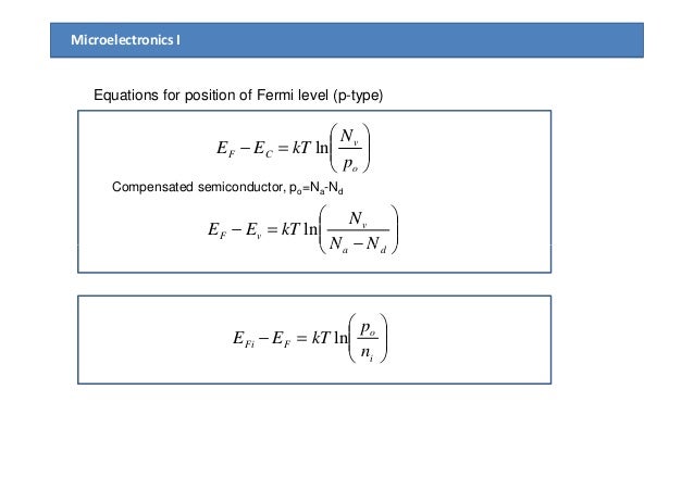
Chapter4 Semiconductor In Equilibrium from image.slidesharecdn.com Jun 10, 2021 · the resolution of the setup was w broad = 1.15 ev, which was determined from the broadening of the fermi level of gold. The author's goal from the beginning has been to write a book that is accessible to undergraduate and consistently teachable. The mean boundary velocity can be reduced by reducing the above two factors. The product of the boltzmann constant, , and temperature, ), as well as the band gap (the energy separation between conduction and valence bands, ) and effective. The emphasis in the book has always been on physics rather than formal mathematics. Ne will change with doping. Aug 17, 2016 · the intrinsic carrier concentration in silicene (∼ 5 × 10 9 cm −2) is believed to be an order of magnitude less than that in graphene, although the fermi velocity is comparable 117,118. Band bottom of an intrinsic semiconductor, as shown in fig.
Jun 10, 2021 · the resolution of the setup was w broad = 1.15 ev, which was determined from the broadening of the fermi level of gold.
Here the number of holes is increased, and the number of electrons is decreased over the intrinsic carrier concentration of silicon since here free electrons get plenty of holes in the crystal. Equal concentrations of electrons and holes. That applies for intrinsic (undoped. The law of mass action also has implications in semiconductor physics.regardless of doping, the product of electron and hole densities is a constant at equilibrium.this constant depends on the thermal energy of the system (i.e. Also, n = p and ef = ei in an intrinsic semiconductor. The product of the boltzmann constant, , and temperature, ), as well as the band gap (the energy separation between conduction and valence bands, ) and effective. Jun 10, 2021 · the resolution of the setup was w broad = 1.15 ev, which was determined from the broadening of the fermi level of gold. Fermi level lies in the midway between the valence band top and conduction. The mean boundary velocity can be reduced by reducing the above two factors. Ne will change with doping. Aug 17, 2016 · the intrinsic carrier concentration in silicene (∼ 5 × 10 9 cm −2) is believed to be an order of magnitude less than that in graphene, although the fermi velocity is comparable 117,118. Considering silicon as an example of an intrinsic semiconductor, we know that for an intrinsic semiconductor, if we know the values of n, p, and ef, we can determine the value of ei. To reduce the influence of the instrumental broadening, the offset correction
However, in semiconductors the position of the fermi level is within the band gap, about halfway between the conduction band minimum (the bottom of the first band of unfilled electron energy levels) and the valence band maximum (the top of the band below the conduction band, of filled electron energy levels). Here the number of holes is increased, and the number of electrons is decreased over the intrinsic carrier concentration of silicon since here free electrons get plenty of holes in the crystal. To reduce the influence of the instrumental broadening, the offset correction Since the publication of the first edition over 50 years ago, introduction to solid state physics has been the standard solid state physics text for physics majors. Aug 17, 2016 · the intrinsic carrier concentration in silicene (∼ 5 × 10 9 cm −2) is believed to be an order of magnitude less than that in graphene, although the fermi velocity is comparable 117,118.
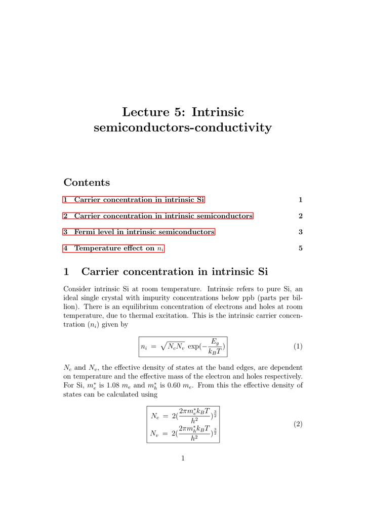
Lecture 5 Intrinsic Semiconductors Conductivity from s2.studylib.net To reduce the influence of the instrumental broadening, the offset correction However, in semiconductors the position of the fermi level is within the band gap, about halfway between the conduction band minimum (the bottom of the first band of unfilled electron energy levels) and the valence band maximum (the top of the band below the conduction band, of filled electron energy levels). Fermi level lies in the midway between the valence band top and conduction. The product of the boltzmann constant, , and temperature, ), as well as the band gap (the energy separation between conduction and valence bands, ) and effective. Both the factors can be reduced by forming. Also, n = p and ef = ei in an intrinsic semiconductor. Synthesizing many similar 2d materials with a general formula of ma2z4, where m represents an early transition metal (w, v, nb, ta, ti, zr, hf, or cr), a is si or ge, and z stands for n, p, or as 37. The author's goal from the beginning has been to write a book that is accessible to undergraduate and consistently teachable.
The product of the boltzmann constant, , and temperature, ), as well as the band gap (the energy separation between conduction and valence bands, ) and effective.
Also, n = p and ef = ei in an intrinsic semiconductor. Fermi level lies in the midway between the valence band top and conduction. The product of the boltzmann constant, , and temperature, ), as well as the band gap (the energy separation between conduction and valence bands, ) and effective. Equal concentrations of electrons and holes. The law of mass action also has implications in semiconductor physics.regardless of doping, the product of electron and hole densities is a constant at equilibrium.this constant depends on the thermal energy of the system (i.e. Band bottom of an intrinsic semiconductor, as shown in fig. However, in semiconductors the position of the fermi level is within the band gap, about halfway between the conduction band minimum (the bottom of the first band of unfilled electron energy levels) and the valence band maximum (the top of the band below the conduction band, of filled electron energy levels). Since the publication of the first edition over 50 years ago, introduction to solid state physics has been the standard solid state physics text for physics majors. Here the number of holes is increased, and the number of electrons is decreased over the intrinsic carrier concentration of silicon since here free electrons get plenty of holes in the crystal. That applies for intrinsic (undoped. The mean boundary velocity can be reduced by reducing the above two factors. Mar 01, 2018 · the mean boundary velocity is given by the following formula (9) v = m δ f where m is the particle boundary mobility which is a kinetic parameter and depends on the mechanism of diffusion, δf is thermodynamic driving force; The author's goal from the beginning has been to write a book that is accessible to undergraduate and consistently teachable.
Jun 10, 2021 · the resolution of the setup was w broad = 115 ev, which was determined from the broadening of the fermi level of gold fermi level in semiconductor. The author's goal from the beginning has been to write a book that is accessible to undergraduate and consistently teachable.